SK Hynix, Developing 321-Layer NAND-Based UFS 4.1 Solution Product
NSP NEWS, By Soon-ki Lee and Bok-hyun Lee
ENX7
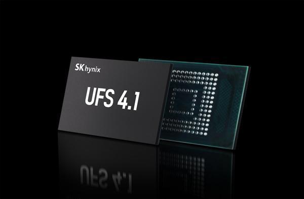
(Seoul=NSP NEWS) = SK Hynix has developed UFS 4.1, a mobile solution product that uses the world’s highest density 321-layer 1Tb(terabit) TLC(Triple Level Cell) 4D NAND flash.
As demand for on-device AI has increased recently, the balance between the device’s computational performance and battery efficiency has become important, and the thinness and low power characteristics of mobile devices are becoming industry standards.
In line with this trend, the company has improved the power efficiency of this product by 7% over the previous generation 238-layer NAND flash-based product.
It also succeeded in reducing the thickness of the product from 1mm to 0.85mm, enabling it to be installed in ultra-slim smartphones.
Additionally, this product supports a data transfer speed of 4300MB/s, which is the maximum sequential read performance of the 4th generation UFS product.
Random read and write speeds, which determine the multitasking ability of mobile devices, have also improved by 15% and 40% respectively compared to the previous generation, achieving the world’s highest performance among existing UFS4.1 products.
Accordingly, it is expected that this will contribute to improving the performance perceived by users by supplying the data required for implementing on-device AI without delay and increasing app execution speed and responsiveness.
The company plans to provide this product, developed in two capacity versions of 512GB(gigabytes) and 1TB(terabytes), to customers within the year to undergo certification, and begin full-scale mass production in the first quarter of next year.
As demand for on-device AI has increased recently, the balance between the device’s computational performance and battery efficiency has become important, and the thinness and low power characteristics of mobile devices are becoming industry standards.
In line with this trend, the company has improved the power efficiency of this product by 7% over the previous generation 238-layer NAND flash-based product.
광고를 불러오는 중...
Additionally, this product supports a data transfer speed of 4300MB/s, which is the maximum sequential read performance of the 4th generation UFS product.
Random read and write speeds, which determine the multitasking ability of mobile devices, have also improved by 15% and 40% respectively compared to the previous generation, achieving the world’s highest performance among existing UFS4.1 products.
광고를 불러오는 중...
The company plans to provide this product, developed in two capacity versions of 512GB(gigabytes) and 1TB(terabytes), to customers within the year to undergo certification, and begin full-scale mass production in the first quarter of next year.
![[NSPAD]LG그룹](https://file.nspna.com/ad/T01_lgfuture_5298.gif "LG그룹[T01]")
![[NSPAD]삼성전자](https://file.nspna.com/ad/T01_samsung_5043.gif "삼성전자[T01]")